
GENERAL
As part of a pulsed energy project, I needed to test a rather large power supply to achieve the desired results (48V @100A). For those that are looking, that’s 5Kw. This article discusses the design & implementation of a hybrid static/transient load testing instrument. This allows static load testing with superimposed transient capability in a single instrument.
For the power supply itself, this will deliver 48v@100A rather easily but will need further characterization. One of the specifications for the power supply is a rigid load transient capability in combination with a large background current.
This required some specialized testing, which required an instrument to perform the following:
- Variable constant current control, 0-1v input = 0-100A load current
- Nominal 48V rating, with a desire to achieve 100V rating if possible.
- Impulse test by pulsing the dc input from baseline to desired current.
- Tr/Tf at the input should be kept fast & tight, typically ~250nsec
- System should be stable under all conditions
- Thermally protected under all conditions
- Step change response to Iset should be reflected by a fast change in Id (~1usec)
There are a couple of high-end instruments that can do this, just not at the power level we want. We looked at paralleling test-sets, etc. but it became excessively expensive. The end result was we recognized the need for an instrument that could handle steady state & pulse loading at high power levels. This work is a genesis of that effort.
BASELINE SPECIFICATIONS
DUT voltage range 48v(min) 100v(preferred)
DUT current range 0-100A 0-100A
Input Range 0-1V (0-100A)
For this evolution I really don’t care about much else. We’re trying to evaluate probabilities of success and want as much flexibility in the design as possible at this point.
PRIOR ART
A search was initiated for similar work, and there were few references to apply linear + pulse loading. Most instruments fall into a category of linear for steady state loading or pulse mode using switching transistors (Mosfet, Bipolar, IGBT). However, we managed to find some work the late great Jim Williams did for LT that was really close to what we were trying to achieve. EDN published an article on this work in the Sept22,2011 edition.
With due apologies to Jim, we branched the design to make it a bit more modern & provide higher voltage capability.
SIMULATION OF PROPOSED DESIGN
To characterize the performance, we modeled a baseline design in LTSpice.
Figure 1- Spice Model
This iteration of the model uses an IXTK200N10P linear mosfet, which limits our voltage capability to 80V or so. However, it’s a good start to evaluate the performance. We ran multiple operating point runs to establish all the bias voltages, and once we had a good scaling established we ran full power pulsing to establish stability.
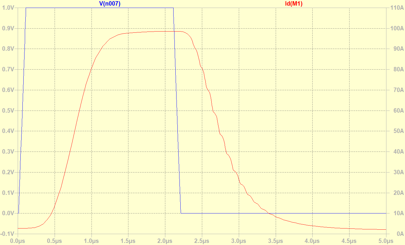
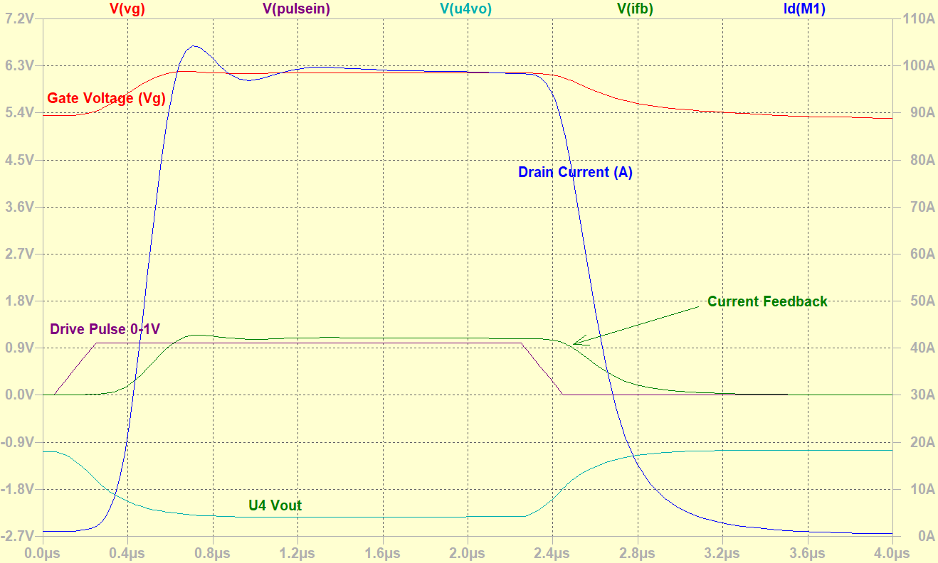
Figure 2- Pulse Response- Full Scale
As can be seen from the plot, transitions are fast & tight (~500nsec tr/tf), with a bit of slight tailing instability. This instability is NOT affected by the loop bandwidth, so its likely a driver stage issue. We may not have quite enough drive capacity in the LT1010, as adding even a small amount of Rg increases the instability. Keeping in mind the stray L could be a factor as well.
Regardless, I’m comfortable with the design approach so far based on the Spice output. Let’s have a look at the drive current on the LT1010 before we close the book.
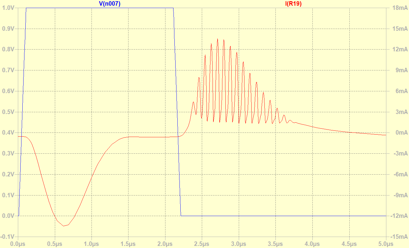
Figure 3- Mosfet Drive Current Instability
Yikes, yup the driver stage is oscillating. As shown in Figure 3, the gate pulse during turn-on looks about o te goal of this effort right but oscillates on turn-off.
When the gate pulse goes high, you can see the driver stage charging the mosfet gate capacitance to a peak of 14ma, and then settles back to zero as the gate is fully charged.
During turn-off, the gate drive starts discharging the gate capacitance but starts oscillating once the discharge current hits ~3ma. Let’s take a look at Vg vs. Ig of the driver stage:
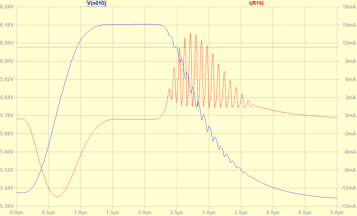
Figure 4- Driver Output Voltage vs. Current
During turn-off, the gate drive starts discharging the gate capacitance but immediately starts going unstable. After evaluating the model, it became apparent the LT1010 driver stage was oscillating. A deep dive into the datasheet (tldr😉) showed I missed a detail about the boost pin. After pulling up the boost pin to V+ through a small R, and most importantly, BYPASSING the pin with a decent cap eliminated the issue. Minor problem, loop stability improved. However, I decided to re-design some bits to give better scaling and push the Tr/Tf limits as far as I could without causing instability. So, let’s look at the revised design in more detail:
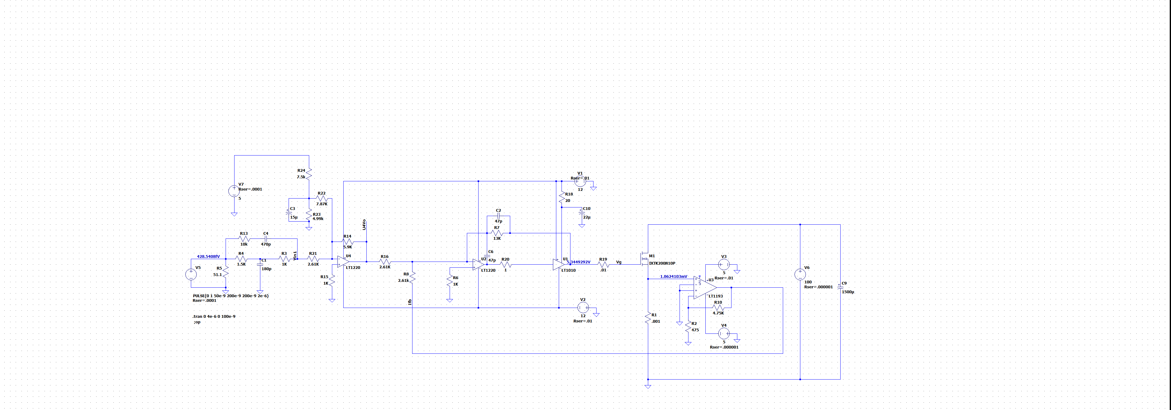
Figure 5 Revision 1 of Model
As seen, the model has been revised in a couple different ways:
- Boost pin has been connected & bypassed for the LT1010
- Moved the gate bias control to U4 instead of U2 to provide better adjustability.
- Optimized the loop bandwidth for sub-microsecond response.
- Eliminated the double termination on the front end.
- Change to a fixed 5V reference for the bias control
Nice. A little peaking on the drain current. Nice fast clean transitions otherwise. Note the ~200nsec Tr/Tf is likely not sustainable in the real world of stray inductances, etc.. but I’m very happy with the results of this run.
SYSTEM CONSIDERATIONS
When taking a larger view of what we hope to accomplish, we have some considerable challenges ahead. It should be obvious we are not going to dump 5KW of power into a single mosfet. This will require multiple paralleled mosfet/driver stages with very careful thermal design. In the next part of this article, we’ll look at Mosfet choices, devices in parallel, how to interpret Mosfet FBSOA curves, and overall thermal design.
It may be useful here to discuss Mosfet linear region operations. Most mosfets are used in switching mode only (fully saturated, Pd set by Rds(on)), and most FBSOA curves for these devices do not include a DC load line. Some previous work has been done to re-characterize some of these devices, with limited success. There are however a limited number of devices on the market specifically designed for linear operation with fully published FBSOA curves including DC. Notable companies such as Infineon, Ixys, Littefuse all manufacture devices characterized for linear operation. In the current model we are using an Ixys IXTK200N10P which is a 200A rated device at 100V. The FBSOA curve for that device is shown below:
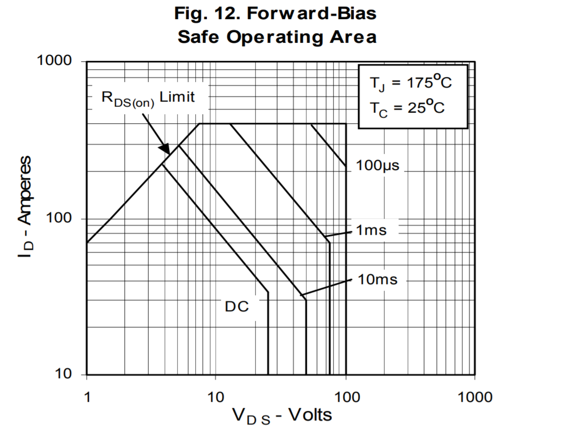
We are limited to around 30V at 25A under DC conditions. Obviously, we have a major issue with supply voltage here that we’ll have to deal with in the next part 2 of the article. (Spoiler alert- yea we have a way to get there).
PATH FORWARD
In order to move the design forward, the following steps will be undertaken in order of significance:
- Detail design of power stage with preliminary selection of power devices. (LTSpice)
- Rerun sims in LTS, evaluate analysis. (LTSpice)
- Run SOA analysis in LTS to determine limits
- Stage Gate- Determine optimum Vmax for the system.
- Port the design to Altium, re-run sims (AD22)
- Detail Design-AD22
- Detailed Thermal Design-AD22/Solidworks/LTS
The spice models for this can be accessed at https://github.com/idewerks/HVAL_Spice
The progress on design will be presented as an 8-part series of articles in the blog.